The Conversation (5)
Sort by

This computer rendering depicts the pattern on a photonic chip that the author and his colleagues have devised for performing neural-network calculations using light.
Think of the many tasks to which computers are being applied that in the not-so-distant past required human intuition. Computers routinely identify objects in images, transcribe speech, translate between languages, diagnose medical conditions, play complex games, and drive cars.
The technique that has empowered these stunning developments is called deep learning, a term that refers to mathematical models known as artificial neural networks. Deep learning is a subfield of machine learning, a branch of computer science based on fitting complex models to data.
While machine learning has been around a long time, deep learning has taken on a life of its own lately. The reason for that has mostly to do with the increasing amounts of computing power that have become widely available—along with the burgeoning quantities of data that can be easily harvested and used to train neural networks.
The amount of computing power at people's fingertips started growing in leaps and bounds at the turn of the millennium, when graphical processing units (GPUs) began to be harnessed for nongraphical calculations, a trend that has become increasingly pervasive over the past decade. But the computing demands of deep learning have been rising even faster. This dynamic has spurred engineers to develop electronic hardware accelerators specifically targeted to deep learning, Google's Tensor Processing Unit (TPU) being a prime example.
Here, I will describe a very different approach to this problem—using optical processors to carry out neural-network calculations with photons instead of electrons. To understand how optics can serve here, you need to know a little bit about how computers currently carry out neural-network calculations. So bear with me as I outline what goes on under the hood.
Almost invariably, artificial neurons are constructed using special software running on digital electronic computers of some sort. That software provides a given neuron with multiple inputs and one output. The state of each neuron depends on the weighted sum of its inputs, to which a nonlinear function, called an activation function, is applied. The result, the output of this neuron, then becomes an input for various other neurons.
For computational efficiency, these neurons are grouped into layers, with neurons connected only to neurons in adjacent layers. The benefit of arranging things that way, as opposed to allowing connections between any two neurons, is that it allows certain mathematical tricks of linear algebra to be used to speed the calculations.
While they are not the whole story, these linear-algebra calculations are the most computationally demanding part of deep learning, particularly as the size of the network grows. This is true for both training (the process of determining what weights to apply to the inputs for each neuron) and for inference (when the neural network is providing the desired results).
What are these mysterious linear-algebra calculations? They aren't so complicated really. They involve operations on matrices, which are just rectangular arrays of numbers—spreadsheets if you will, minus the descriptive column headers you might find in a typical Excel file.
This is great news because modern computer hardware has been very well optimized for matrix operations, which were the bread and butter of high-performance computing long before deep learning became popular. The relevant matrix calculations for deep learning boil down to a large number of multiply-and-accumulate operations, whereby pairs of numbers are multiplied together and their products are added up.
 Two beams whose electric fields are proportional to the numbers to be multiplied, x and y, impinge on a beam splitter (blue square). The beams leaving the beam splitter shine on photodetectors (ovals), which provide electrical signals proportional to these electric fields squared. Inverting one photodetector signal and adding it to the other then results in a signal proportional to the product of the two inputs.David Schneider
Over the years, deep learning has required an ever-growing number of these multiply-and-accumulate operations. Consider LeNet, a pioneering deep neural network, designed to do image classification. In 1998 it was shown to outperform other machine techniques for recognizing handwritten letters and numerals. But by 2012 AlexNet, a neural network that crunched through about 1,600 times as many multiply-and-accumulate operations as LeNet, was able to recognize thousands of different types of objects in images.
Advancing from LeNet's initial success to AlexNet required almost 11 doublings of computing performance. During the 14 years that took, Moore's law provided much of that increase. The challenge has been to keep this trend going now that Moore's law is running out of steam. The usual solution is simply to throw more computing resources—along with time, money, and energy—at the problem.
As a result, training today's large neural networks often has a significant environmental footprint. One 2019 study found, for example, that training a certain deep neural network for natural-language processing produced five times the CO2 emissions typically associated with driving an automobile over its lifetime.
Improvements in digital electronic computers allowed deep learning to blossom, to be sure. But that doesn't mean that the only way to carry out neural-network calculations is with such machines. Decades ago, when digital computers were still relatively primitive, some engineers tackled difficult calculations using analog computers instead. As digital electronics improved, those analog computers fell by the wayside. But it may be time to pursue that strategy once again, in particular when the analog computations can be done optically.
It has long been known that optical fibers can support much higher data rates than electrical wires. That's why all long-haul communication lines went optical, starting in the late 1970s. Since then, optical data links have replaced copper wires for shorter and shorter spans, all the way down to rack-to-rack communication in data centers. Optical data communication is faster and uses less power. Optical computing promises the same advantages.
But there is a big difference between communicating data and computing with it. And this is where analog optical approaches hit a roadblock. Conventional computers are based on transistors, which are highly nonlinear circuit elements—meaning that their outputs aren't just proportional to their inputs, at least when used for computing. Nonlinearity is what lets transistors switch on and off, allowing them to be fashioned into logic gates. This switching is easy to accomplish with electronics, for which nonlinearities are a dime a dozen. But photons follow Maxwell's equations, which are annoyingly linear, meaning that the output of an optical device is typically proportional to its inputs.
The trick is to use the linearity of optical devices to do the one thing that deep learning relies on most: linear algebra.
To illustrate how that can be done, I'll describe here a photonic device that, when coupled to some simple analog electronics, can multiply two matrices together. Such multiplication combines the rows of one matrix with the columns of the other. More precisely, it multiplies pairs of numbers from these rows and columns and adds their products together—the multiply-and-accumulate operations I described earlier. My MIT colleagues and I published a paper about how this could be done in 2019. We're working now to build such an optical matrix multiplier.
The basic computing unit in this device is an optical element called a beam splitter. Although its makeup is in fact more complicated, you can think of it as a half-silvered mirror set at a 45-degree angle. If you send a beam of light into it from the side, the beam splitter will allow half that light to pass straight through it, while the other half is reflected from the angled mirror, causing it to bounce off at 90 degrees from the incoming beam.
Now shine a second beam of light, perpendicular to the first, into this beam splitter so that it impinges on the other side of the angled mirror. Half of this second beam will similarly be transmitted and half reflected at 90 degrees. The two output beams will combine with the two outputs from the first beam. So this beam splitter has two inputs and two outputs.
To use this device for matrix multiplication, you generate two light beams with electric-field intensities that are proportional to the two numbers you want to multiply. Let's call these field intensities x and y. Shine those two beams into the beam splitter, which will combine these two beams. This particular beam splitter does that in a way that will produce two outputs whose electric fields have values of (x + y)/√2 and (x − y)/√2.
In addition to the beam splitter, this analog multiplier requires two simple electronic components—photodetectors—to measure the two output beams. They don't measure the electric field intensity of those beams, though. They measure the power of a beam, which is proportional to the square of its electric-field intensity.
Why is that relation important? To understand that requires some algebra—but nothing beyond what you learned in high school. Recall that when you square ( x + y)/√2 you get (x2 + 2xy + y2)/2. And when you square (x − y)/√2, you get (x2 − 2xy + y2)/2. Subtracting the latter from the former gives 2xy.
Pause now to contemplate the significance of this simple bit of math. It means that if you encode a number as a beam of light of a certain intensity and another number as a beam of another intensity, send them through such a beam splitter, measure the two outputs with photodetectors, and negate one of the resulting electrical signals before summing them together, you will have a signal proportional to the product of your two numbers.
My description has made it sound as though each of these light beams must be held steady. In fact, you can briefly pulse the light in the two input beams and measure the output pulse. Better yet, you can feed the output signal into a capacitor, which will then accumulate charge for as long as the pulse lasts. Then you can pulse the inputs again for the same duration, this time encoding two new numbers to be multiplied together. Their product adds some more charge to the capacitor. You can repeat this process as many times as you like, each time carrying out another multiply-and-accumulate operation.
Using pulsed light in this way allows you to perform many such operations in rapid-fire sequence. The most energy-intensive part of all this is reading the voltage on that capacitor, which requires an analog-to-digital converter. But you don't have to do that after each pulse—you can wait until the end of a sequence of, say, N pulses. That means that the device can perform N multiply-and-accumulate operations using the same amount of energy to read the answer whether N is small or large. Here, N corresponds to the number of neurons per layer in your neural network, which can easily number in the thousands. So this strategy uses very little energy.
Sometimes you can save energy on the input side of things, too. That's because the same value is often used as an input to multiple neurons. Rather than that number being converted into light multiple times—consuming energy each time—it can be transformed just once, and the light beam that is created can be split into many channels. In this way, the energy cost of input conversion is amortized over many operations.
Splitting one beam into many channels requires nothing more complicated than a lens, but lenses can be tricky to put onto a chip. So the device we are developing to perform neural-network calculations optically may well end up being a hybrid that combines highly integrated photonic chips with separate optical elements.
I've outlined here the strategy my colleagues and I have been pursuing, but there are other ways to skin an optical cat. Another promising scheme is based on something called a Mach-Zehnder interferometer, which combines two beam splitters and two fully reflecting mirrors. It, too, can be used to carry out matrix multiplication optically. Two MIT-based startups, Lightmatter and Lightelligence, are developing optical neural-network accelerators based on this approach. Lightmatter has already built a prototype that uses an optical chip it has fabricated. And the company expects to begin selling an optical accelerator board that uses that chip later this year.
Another startup using optics for computing is Optalysis, which hopes to revive a rather old concept. One of the first uses of optical computing back in the 1960s was for the processing of synthetic-aperture radar data. A key part of the challenge was to apply to the measured data a mathematical operation called the Fourier transform. Digital computers of the time struggled with such things. Even now, applying the Fourier transform to large amounts of data can be computationally intensive. But a Fourier transform can be carried out optically with nothing more complicated than a lens, which for some years was how engineers processed synthetic-aperture data. Optalysis hopes to bring this approach up to date and apply it more widely.
There is also a company called Luminous, spun out of Princeton University, which is working to create spiking neural networks based on something it calls a laser neuron. Spiking neural networks more closely mimic how biological neural networks work and, like our own brains, are able to compute using very little energy. Luminous's hardware is still in the early phase of development, but the promise of combining two energy-saving approaches—spiking and optics—is quite exciting.
There are, of course, still many technical challenges to be overcome. One is to improve the accuracy and dynamic range of the analog optical calculations, which are nowhere near as good as what can be achieved with digital electronics. That's because these optical processors suffer from various sources of noise and because the digital-to-analog and analog-to-digital converters used to get the data in and out are of limited accuracy. Indeed, it's difficult to imagine an optical neural network operating with more than 8 to 10 bits of precision. While 8-bit electronic deep-learning hardware exists (the Google TPU is a good example), this industry demands higher precision, especially for neural-network training.
There is also the difficulty integrating optical components onto a chip. Because those components are tens of micrometers in size, they can't be packed nearly as tightly as transistors, so the required chip area adds up quickly. A 2017 demonstration of this approach by MIT researchers involved a chip that was 1.5 millimeters on a side. Even the biggest chips are no larger than several square centimeters, which places limits on the sizes of matrices that can be processed in parallel this way.
There are many additional questions on the computer-architecture side that photonics researchers tend to sweep under the rug. What's clear though is that, at least theoretically, photonics has the potential to accelerate deep learning by several orders of magnitude.
Based on the technology that's currently available for the various components (optical modulators, detectors, amplifiers, analog-to-digital converters), it's reasonable to think that the energy efficiency of neural-network calculations could be made 1,000 times better than today's electronic processors. Making more aggressive assumptions about emerging optical technology, that factor might be as large as a million. And because electronic processors are power-limited, these improvements in energy efficiency will likely translate into corresponding improvements in speed.
Many of the concepts in analog optical computing are decades old. Some even predate silicon computers. Schemes for optical matrix multiplication, and even for optical neural networks, were first demonstrated in the 1970s. But this approach didn't catch on. Will this time be different? Possibly, for three reasons.
First, deep learning is genuinely useful now, not just an academic curiosity. Second, we can't rely on Moore's Law alone to continue improving electronics. And finally, we have a new technology that was not available to earlier generations: integrated photonics. These factors suggest that optical neural networks will arrive for real this time—and the future of such computations may indeed be photonic.

Nuclear energy has fallen off the radar screen since September, when the Russian-occupied Zaporizhzhia nuclear plant finally shut down. But Ukraine’s reliance on the three nuclear plants still operating—as well as their vulnerability—has never been higher.
A letter from a prominent member of Ukraine’s nuclear establishment warns of an “emerging critical situation” with “catastrophic” implications for Ukraine’s defense.
Ukraine has lost 75 percent of its coal- and gas-fired power plants, and Zaporizhzhia was its largest nuclear generator. That leaves Ukraine extraordinarily dependent on the three remaining nuclear power stations—the Rivne, Khmelnytskyi and South Ukraine plants. Before the invasion, those plants’ nine reactors supplied one-quarter of Ukraine’s electricity. Now they provide at least half.
The nuclear plants face a perpetual threat of Russian attack, as well as damage to their turbine generators when Russia’s persistent bombardment of substations causes AC power fluctuations. Power glitches tossed one of Khmelnytsky’s units offline last month.
Keeping reactors fueled may pose an even bigger challenge. Ukraine is running short of fresh fuel, which must be swapped in in every 12 months. Meanwhile, spent fuel backing up at the plants is complicating those swaps.
Petro Kotin, CEO of Ukraine’s state-owned nuclear power company, Energoatom, brushed aside fuel concerns in January, telling Bloomberg that Ukraine has “several years’ worth of fuel” on hand. But his reassurances have faced pushback.
One Ukrainian nuclear expert says only “extraordinary measures” can keep Ukraine from losing thousands of megawatts of nuclear output. Another, a former secretary of Ukraine’s parliamentary energy committee, Victoria Voytsitska, was in Washington, D.C., this week pleading for help from Congress and federal agencies to secure Ukraine’s fuel supply.
Voytsitska’s message is that Ukraine is running out of time: “Our ability to survive and win this war is directly linked [to] and dependent on...generating enough electricity.”
Catastrophic shortfalls ahead?
Refueling concerns began spreading thanks to a letter written last month by Nikolai Steinberg, an éminence grise of Ukraine’s nuclear energy establishment, who was once chief engineer at Chernobyl and a governing director of the International Atomic Energy Agency. Steinberg’s letter, circulated to colleagues and seen by IEEE Spectrum, warns of an “emerging critical situation” with “catastrophic” implications for Ukraine’s defense.
Ukraine and most other European countries with Russian-design reactors use fuel from the Moscow-based nuclear-energy giant Rosatom. Pittsburgh-based Westinghouse Electric is their only alternative fuel supplier, and demand far outstrips its supply.
Steinberg based his concerns on an assessment by Ukrainian nuclear experts that reviewed fuel availability from Westinghouse, as well as equipment needed to upgrade reactor controls and instrumentation to use that fuel.
One former Energoatom official is already under house arrest for allegedly fraudulent power sales in 2020.
“Our staff has relevant experience. The question is the availability of components,” stated Steinberg in an email exchange with IEEE Spectrum last week.
Steinberg’s letter states that, without the required supplies, Energoatom stands to lose 2,400 megawatts of nuclear generating capacity this year, and a further 4,000 MW in 2024.
Pavlo Pavlyshyn, former director of the Rivne Nuclear Power Plant, calls Steinberg’s warning “important.” Now deputy mayor of nearby Varash, Pavlyshyn says the fuel on-site will sustain only one of its two 440-MW reactors this year.
Westinghouse makes fuel for Ukraine’s 1,000-MW plants, but it must revive a plant in Sweden to supply Rivne’s smaller reactors. That fuel isn’t expected to begin shipping until early 2024. Plus, it was designed for a slightly different kind of reactor and therefore must first be cleared for use at Rivne.
Energoatom insists that all of its nuclear power units will be “supplied” with Westinghouse fuel “starting from 2024.”
And then there’s the overcrowding at reactor fuel pools. That congestion could still stall the refueling effort, even if Energoatom efficiently upgrades and relicenses its reactors and Westinghouse delivers sufficient fuel in time.
Historically, Energoatom maintained free pool space by shipping partially cooled fuel to Russia for processing every time it added superheated fuel to a pool. But it paused fuel removals in anticipation of a storage facility under construction at Chernobyl, beside the Belorussian border north of Kyiv. “Almost no spent fuel was removed for several years,” said Steinberg.
 Spent fuel storage containers are seen at Chernobyl.Energoatom
After several years’ delay and premature declarations of the facility’s completion by Energoatom CEO Kotin and Minister of Energy German Galushchenko, Kotin once again declared the company ready to take fuel shipments early last year. Unfortunately, by then its readiness was irrelevant. Shipping canisters of highly radioactive material weighing up to 200 tonnes is considered unsafe amid Russia’s aerial barrages—especially deliveries to the Chernobyl area that Russian troops overran within hours last February.
Energoatom now seeks a regulatory sign-off to put spent fuel in shipping canisters and temporarily tuck them into the corridors of reactor containment buildings, according to a Ukrainian nuclear expert contacted by Spectrum. “For one year it is justified,” he says.
Voytsitska says Ukraine needs better air defenses to transport both fresh and spent fuel, and to secure its spent fuel storage facility. “The storage facility at Chernobyl has to become operational and for that we need extra protection,” she says.
Voytsitska notes that international partners secured the deal to safely move Ukraine’s grain. She says they must also help Ukraine move nuclear fuel.
Energoatom’s head in the game?
Steinberg said he circulated his letter hoping that someone would convey his concerns to Ukraine’s “senior leadership,” expressing doubt that Energoatom or the Ministry of Energy would inform them of the “true state of affairs.” His doubts are not unique. Kotin and other Energoatom executives, as well as energy minister Galushchenko, face revived and expanded allegations of corruption and Russian influence.
One former official appointed under Kotin’s watch is already under house arrest for allegedly fraudulent power sales in 2020. And additional allegations of irregular electricity sales since the invasion may have weakened Energoatom’s reactor refueling program.
Spectrum covered scrutiny of Kotin and his team last March and July. Questions resurfaced this January after a series of high-profile firings by President Zelenskyy. Energoatom personnel director Oleg Boyarintsev fled the country two days later, according to a Facebook post by longtime Kotin critic Olga Kosharna. Sources contacted by Spectrum independently confirm Boyarintsev’s departure.
 Petro Kotin, CEO of Energoatom, sits during a visit to the Chernobyl storage site.Energoatom
In mid-February, Kosharna added that both Boyarintsev and Energoatom security chief Sergey Rossokha had resigned. Energoatom says they “voluntarily resigned.”
Ukraine’s High Anti-Corruption Court weighed in last month, placing another former Energoatom official under house detention. Government investigators allege that fraudulent power sales in 2020 by the former director of energy trading, Aleksey Statnik, cost the utility UAH 93.76 million (US $2.55 million). The winning bidder passed the electricity to steel plants owned by Ukrainian oligarch Igor Kolomoisky, who also faces scrutiny by investigators.
Statnik could, however, be taking the fall for higher-ups, based on reporting by Kyiv-based energy news outlet Kosatka Media in 2021.
Kosatka Media documented that Statnik, hired in September and fired in October, was the last in a string of revolving Energoatom trading directors. It quoted the utility’s former anticorruption officer Oleh Polishchuk explaining that Statnik ran afoul of Energoatom finance chief Hartmut Jacob by refusing to execute Jacob’s “dubious instructions on the sale of electricity.”
The article included a 9 October 2020 memo from Statnik documenting how illogical trades were bleeding Energoatom’s coffers. After that memo—and mere weeks on the job— Statnik was sent on vacation, according to Polishchuk’s account. At which point Jacob, with Kotin’s authorization, personally executed more money-losing trades.
Energoatom eliminated Statnik’s position before he returned from vacation. Polishchuk himself was dismissed by Boyarintsev and Kotin after he questioned the trades as well as bonuses paid to Jacob and energy minister Galushchenko, who was then an Energoatom vice president; a Ukrainian judge deemed his dismissal illegal.
The link between dodgy trades and Energoatom’s refueling challenges appear in separate allegations by Viktor Kurtiev, a Ukrainian energy expert and entrepreneur. Kurtiev asserts in a December 2022 that the Ministry of Energy and Energoatom organized a shell game last year that diverted part of a UAH 1.5 billion loan secured by Energoatom for the purchase of Westinghouse fuel.
According to documents Kurtiev obtained, Energoatom handed one-third of those funds to another state firm so that it could buy power from Energoatom and export it to Europe. That state firm, Kurtiev alleges, then shared its export rights with a private trader. The net result, Kurtiev tells Spectrum, was that both Energoatom and the state trading firm appear to have lost money on profitable sales.
In an email response, Energoatom says that it trades “according to the Law of Ukraine on the Electric Energy Market.” It adds that “Currently, Energoatom fully cooperates with law enforcement authorities.”
What’s most damaging, if the allegations are proven, is how Energoatom generated surplus power to export: by ignoring safety experts and operating its embattled Zaporizhzhia nuclear plant amid hostile fire and repeated blackouts.
What’s most bizarre is the fact that Energoatom could have simply executed the sales itself, earning profits that it could now be using to buy fuel.
Global Configuration Management - The Game Changer for Requirements Management
In this presentation we will build the case for component-based requirements management, illustrate Global Configuration Management concepts, and focus on various Component Usage Patterns within the context of GCM 7.0.2 and IBM’s Engineering Lifecycle (ELM) suite of tools.
Before GCM, Project Areas were the only containers available for organizing data. Project Areas could support only one stream of development. Enabling application local Configuration Management (CM) and GCM allows for the use of Components. Components are contained within Project Areas and provide more granular containers for organizing artifacts and new configuration management constructs; streams, baselines, and change sets at the local and global levels. Components can be used to organize requirements either functionally, logically, physically, or using some combination of the three. A stream identifies the latest version of a modifiable configuration of every artifact housed in a component. The stream automatically updates the configuration as new versions of artifacts are created in the context of the stream. The multiple stream capability in components equips teams the tools needed to seamlessly manage multiple releases or variants within a single component.
GCM arms product/system development organizations with support for advanced requirement reuse, traceability that supports versioning, release management, and variant management.
Prior to GCM support, the associations between Project Areas would enable traceability between single version of ALM artifacts. With GCM, virtual networks of components can be constructed allowing for traceability between artifacts across components – between requirements components and between artifacts across other ALM domains (software, change management, testing, modeling, product parts, etc.).
321 Gang has defined common usage patterns for working with components and their streams. These patterns include Variant Development, Parallel Release Management, Simple Single Stream Development, and others. The GCM capability for virtual networks and the use of some of these patterns provide a foundation to support PLE.
The 321 Gang has put together a short webinar also titled Global Configuration Management: A Game Changer for Requirements Management, that expands on the topics discussed here. During the webinar we build a case for component-based requirements management, illustrate Global Configuration Management concepts, and introduce common GCM usage patterns using ELM suite of tools. Watch this on-demand webinar now.


A researcher at IBM’s Thomas J. Watson Research Center examines some of the quantum hardware being constructed there.
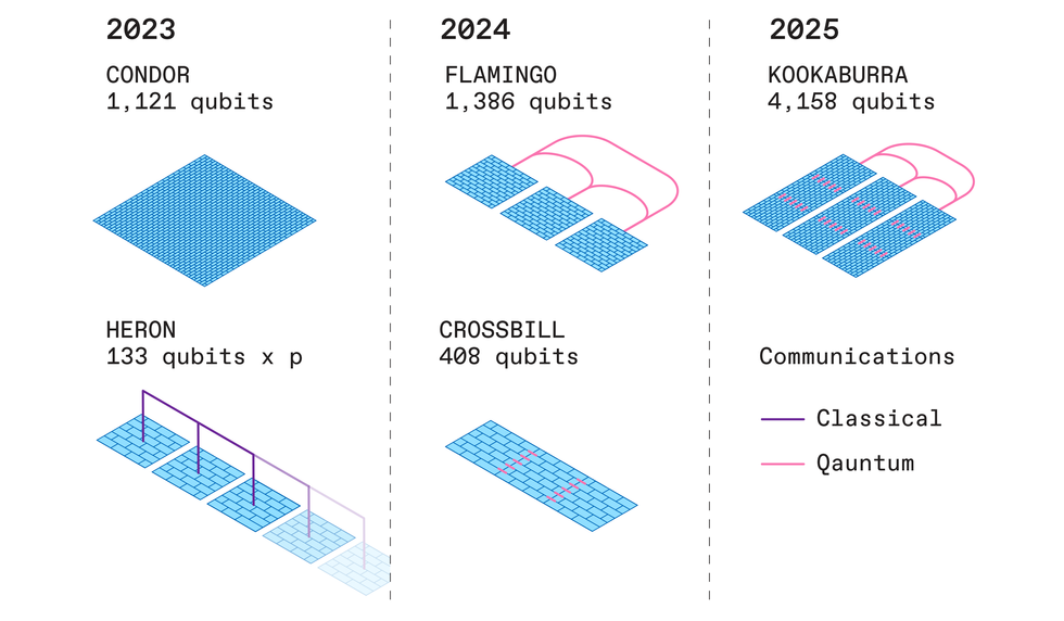
Nevertheless, IBM has steadily increased its qubit numbers. In 2016, it put the first quantum computer in the cloud anyone to experiment with—a device with 5 qubits, each a superconducting circuit cooled to near absolute zero. In 2019, the company created the 27-qubit Falcon; in 2020, the 65-qubit Hummingbird; in 2021, the 127-qubit Eagle, the first quantum processor with more than 100 qubits; and in 2022, the 433-qubit Osprey.
 IBM expects to build quantum computers of increasing complexity over the next few years, starting with those that use the Condor processor or multiple Heron processors in parallel.Carl De Torres/IBM
Other quantum computers have more qubits than does IBM’s 1,121-qubit Condor processor—for instance, D-Wave Systems unveiled a 5,000-qubit system in 2020. But D-Wave’s computers are specialized machines for solving optimization problems, whereas Condor will be the world’s largest general-purpose quantum processor.
“A thousand qubits really pushes the envelope in terms of what we can really integrate,” says Jerry Chow, IBM’s director of quantum infrastructure. By separating the wires and other components needed for readout and control onto their own layers, a strategy that began with Eagle, the researchers say they can better protect qubits from disruption and incorporate larger numbers of them. “As we scale upwards, we’re learning design rules like ‘This can go over this; this can’t go over this; this space can be used for this task,’” Chow says.
Other quantum computers with more qubits exist, but Condor will be the world’s largest general-purpose quantum processor.
With only 133 qubits, Heron, the other quantum processor IBM plans for 2023, may seem modest compared with Condor. But IBM says its upgraded architecture and modular design herald a new strategy for developing powerful quantum computers. Whereas Condor uses a fixed-coupling architecture to connect its qubits, Heron will use a tunable-coupling architecture, which adds Josephson junctions between the superconducting loops that carry the qubits. This strategy reduces crosstalk between qubits, boosting processing speed and reducing errors. Google e is already using such an architecture with its 53-qubit Sycamore processor.)
In addition, Heron processors are designed for real-time classical communication with one another. The classical nature of these links means their qubits cannot entangle across Heron chips for the kind of boosts in computing power for which quantum processors are known. Still, these classical links enable “ circuit knitting” techniques in which quantum computers can get assistance from classical computers.
For example, using a technique known as “ entanglement forging,” IBM researchers found they could simulate quantum systems such as molecules using only half as many qubits as is typically needed. This approach divides a quantum system into two halves, models each half separately on a quantum computer, and then uses classical computing to calculate the entanglement between both halves and knit the models together.
IBM Quantum State of the Union 2022
While these classical links between processors are helpful, IBM intends eventually to replace them. In 2024, the company aims to launch Crossbill, a 408-qubit processor made from three microchips coupled together by short-range quantum communication links, and Flamingo, a 462-qubit module it plans on uniting by roughly 1-meter-long quantum communication links into a 1,386-qubit system. If these experiments in connectivity succeed, IBM aims to unveil its 1,386-qubit Kookaburra module in 2025, with short- and long-range quantum communication links combining three such modules into a 4,158-qubit system.
IBM’s methodical strategy of “aiming at step-by-step improvements is very reasonable, and it will likely lead to success over the long term,” says Franco Nori, chief scientist at the Theoretical Quantum Physics Laboratory at the Riken research institute in Japan.
In 2023, IBM also plans to improve its core software to help developers use quantum and classical computing in unison over the cloud. “We’re laying the groundwork for what a quantum-centric supercomputer looks like,” Chow says. “We don’t see quantum processors as fully integrated but as loosely aggregated.” This kind of framework will grant the flexibility needed to accommodate the constant upgrades that quantum hardware and software will likely experience, he explains.
In 2023, IBM plans to begin prototyping quantum software applications. By 2025, the company expects to introduce such applications in machine learning, optimization problems, the natural sciences, and beyond.
Researchers hope ultimately to use quantum error correction to compensate for the mistakes quantum processors are prone to make. These schemes spread quantum data across redundant qubits, requiring multiple physical qubits for each single useful logical qubit. Instead, IBM plans to incorporate error-mitigation schemes into its platform starting in 2024, to prevent these mistakes in the first place. But even if wrangling errors ends up demanding many more qubits, IBM should be in a good position with the likes of its 1,121-qubit Condor.
This article appears in the January 2023 print issue as “IBM’s Quantum Leap .”